

Introduction
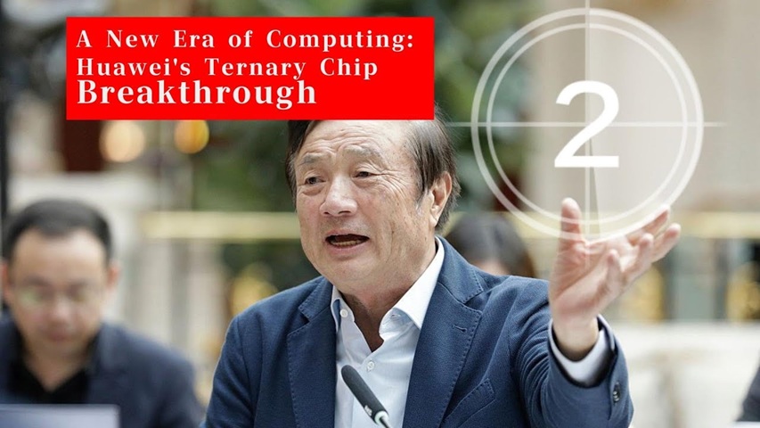
A groundbreaking development today (2025) in computing technology as Huawei officially unveils the world’s first ternary logic chip, marking a potential paradigm shift that could end the 80-year dominance of binary computing systems. The announcement represents not just a technical achievement, but a geopolitical milestone that demonstrates how technological innovation can emerge from unexpected quarters, particularly amid ongoing global tech tensions.
About the Ternary Chip
Technical Specifications
Core Architecture
Huawei’s breakthrough lies in the stable operation of ternary logic gates through a fully digital CMOS architecture. Its core innovations include: using threshold voltage layering technology to map input signals to 0V (0), 1.65V (+1), and 3.3V (-1), and implementing addition and subtraction operations through transistor combination logic
Key Technical Specifications:
- Logic States: Three-state system using -1, 0, and +1 instead of binary 0 and 1
- Voltage Mapping:
- 0V represents logic state “0”
- 1.65V represents logic state “+1”
- 3.3V represents logic state “-1”
- Process Technology: 7nm process, which is three times that of traditional binary GPUs
- Energy Efficiency: 1.8TOPS/W under the 7nm process
- Error Rate: controls voltage fluctuations within ±50mV by optimizing the gate structure
Performance Metrics
Huawei’s ternary logic gate achieves performance breakthroughs through the following innovations: Dynamic power consumption optimization: The number of transistors is reduced by 40%, and the dynamic power consumption is reduced to 1/3 of that of binary circuits
Efficiency Improvements:
- 40% fewer transistors required compared to binary systems
- 60% reduction in power consumption
- 20% shorter critical path delay through path parallelization design
- Information density advantage: the decimal number 128 requires 8 bits of binary representation, while ternary only requires 5 bits
Advanced Design Architecture
Carbon Nanotube Field-Effect Transistor (CNTFET) Implementation
The patent also mentions the use of CNTFET (carbon nanotube field-effect transistors), which offer advantages that could enable precise voltage control for ternary systems
Design Features:
- Multi-threshold voltage capability: CNTFETs are currently being preferred for implementing ternary circuits due to their desirable multiple threshold voltage and geometry-dependent properties
- Precise voltage control: CNTFETs have the capability of having the desired threshold voltage by changing the diameters of the nanotubes, which make them a very suitable device for voltage mode multiple threshold circuit design
- Enhanced stability: Due to its unique 1D band structure, CNTFET has near-ballistic transport operation, thereby providing exceptional driving capability and lesser power dissipation
Quantum State Isolated Gate Technology
The chip incorporates proprietary quantum state isolated gate technology with:
- Multi-layered nanoscale insulating materials
- Custom-designed logic gate circuits
- Signal cross-talk problem resolution that plagued earlier ternary systems
- Error rate control: Less than 0.00001% misjudgment rate for the three logic states
Integration with Resistive RAM (ReRAM)
Storage and computing integration: When combined with ReRAM, the energy efficiency of in-memory computing can reach 4.2 times that of traditional architectures
Video introduction of ternary logic chip
Key Sections of this Video
Understanding Ternary Logic: The Technical Revolution
The video explains that traditional computing operates on binary logic with two states (on/off), similar to a light switch. Huawei’s breakthrough introduces a third “half-on” state, working with three states: minus-1, 0, and +1. This seemingly simple addition creates dramatic efficiency improvements.
Key Technical Advantages:
- Doubled efficiency: A traffic light system requiring three transistors in binary can operate with just one transistor in ternary
- 60% increase in computing power for equivalent tasks
- More than 50% reduction in power consumption
- Enhanced security: The system is nearly impervious to malware infiltration due to its inherent stability
The video uses an effective analogy, comparing this advance to “widening a two-lane road to three lanes” where information flows faster with less effort.
Historical Context: Soviet Ambitions vs. Modern Success
The narrative provides fascinating historical context, revealing how Soviet scientists in 1958 built the world’s first ternary computer called “Satin” under Nikolai Brazens at Moscow State University. Despite initial promise and superior speed compared to binary computers, the project ultimately failed due to hardware reliability issues – the system couldn’t reliably distinguish the half-on state, especially during temperature fluctuations.
Huawei’s Solution:
- Quantum state isolated gate technology with custom-designed logic circuits
- Multi-layered nanoscale insulating materials creating stable signal isolation
- Error rate of less than 0.00001% for distinguishing between the three states
- Complete ecosystem integration from chip to software, unlike the Soviet’s hardware-only approach
The Tech War and Unintended Consequences
The video frames Huawei’s breakthrough within the context of ongoing US-China tech tensions, highlighting how semiconductor blockades have created unexpected outcomes. The analysis shows that US export controls, rather than weakening competitors, have accelerated innovation and self-reliance.
Market Impact Examples:
- Nvidia’s revenue in China plummeted by over $11 billion within six months of tightened controls
- Stock price dropped over 20%, forcing CEO Jensen Huang to publicly advocate for restored exports
- The restrictions have democratized AI development, making it accessible to smaller companies and research institutions
Future Implications and Ecosystem Building
Unlike the Soviet approach that focused solely on hardware, Huawei has built a comprehensive technological ecosystem:
- Ascend AI platform with 300% improved parallel processing efficiency
- Harmony OS with ternary interface support since version 2.0
- Complete supply chain involving over 1,000 domestic suppliers
- Vertical integration from chip design to end-user applications
The video emphasizes that this represents more than incremental improvement – it’s a fundamental restructuring of computing architecture that could reshape global tech competition.
The Real-World Applications
AI and Data Center Applications
these energy-efficient AI chipsets will further be useful for data centers equipped with powerful GPUs and requires a lot of power in one go
Specific Use Cases:
- Large Language Model Training: Potential to reduce training costs similar to OpenAI’s GPT training by 50%
- AI Inference: Huawei’s HiSilicon Ascend 910C is part of the Ascend 910 family of chips introduced in 2019. Due to sanctions, AI labs in China can not buy the newest highest performance chips from US firms like NVIDIA or AMD
- Edge Computing: After combining with storage and computing technology, the energy consumption of data transfer is reduced by 90%, and the endurance of equipment increases exponentially
Automotive Industry Applications
Experimental data show that for a server cluster equipped with a ternary accelerator card, the electricity cost per thousand inferences in an autonomous driving training scenario is reduced from 0.03 yuan to 0.01 yuan. For automakers that perform an average of 1 trillion operations per day, this can save hundreds of millions of yuan in costs each year
Automotive Benefits:
- 67% cost reduction in autonomous driving computations
- Enhanced efficiency for real-time processing requirements
- Improved energy management for electric vehicles
Machine Learning and Model Training
Model training: When processing the ResNet-50 model, training time was reduced by 28% and electricity costs were reduced by 42%
ML Applications:
- Computer Vision: Improved performance in image recognition tasks
- Natural Language Processing: Enhanced efficiency in transformer models
- Approximate Computing: Dynamically switch between precise and approximate modes during AI training, maintaining 95% computing accuracy while reducing energy consumption by 40%
Quantum Computing Compatibility
Quantum compatibility: Symmetrical logic systems are naturally compatible with the superposition state characteristics of quantum bits, and the quantum-ternary interface design can reduce error correction costs by 60%
Commercial Implementation and Ecosystem Integration
Harmony OS Integration
The chip is designed to work seamlessly with Huawei’s ecosystem:
- Harmony OS 2.0 includes ternary OS interface reserves
- Ascend AI platform integration with 300% improved parallel processing efficiency
- Complete supply chain involving over 1,000 domestic suppliers
Patent and Development Timeline
- Patent Filed: September 2023 (CN119652311A)
- Patent Published: March 2025
- Lead Scientists: Hu Hailin and Huang Mingqiang
- Commercial Viability: While promising, CNTFET technology is still immature and far from commercialization. Huawei’s patent is seen as a technological reserve
Competitive Advantages and Market Impact
Power Efficiency Breakthrough
Traditional binary GPUs require 200W of power to achieve 30 TFLOPS computing power, while ternary chips only require 75W to achieve the same performance
Information Density Revolution
Three ternary bits can represent 27 states, compared to 8 states for three binary bits, providing higher information density and reduced storage requirements.
Manufacturing Cost Benefits
The technology addresses current semiconductor industry challenges by potentially bypassing the need for advanced manufacturing processes through increased information density rather than smaller transistor sizes.
Key Advantages:
- Miniaturization through logic rather than manufacturing advancement
- Reduced interconnect complexity
- Lower heat generation and cooling requirements
- Enhanced security through inherent system stability
Conclusion and Key Takeaways
Huawei’s ternary logic chip represents a fundamental shift from incremental improvements to architectural innovation, potentially establishing a new paradigm in computing that could influence everything from smartphones to supercomputers. The technology’s success will largely depend on ecosystem adoption and manufacturing scalability over the coming years.
Major Takeaways:
- Paradigm Shift: Huawei’s ternary chip represents the first serious challenge to binary computing’s 80-year dominance, offering significant efficiency and power consumption improvements.
- Historical Vindication: The success where Soviet scientists failed demonstrates the importance of ecosystem thinking over isolated technological breakthroughs.
- Geopolitical Impact: The breakthrough illustrates how tech restrictions can accelerate rather than hinder innovation, creating stronger, more self-reliant technological capabilities.
- Democratization of AI: With dramatically reduced computing costs, AI development becomes accessible to a broader range of organizations, potentially spurring unprecedented innovation.
- Strategic Lesson: The contrast between Soviet state-controlled innovation and Huawei’s market-integrated approach highlights the crucial role of ecosystem building in technological success.
This development represents not just a technical achievement, but “a ripple in the pond of global technology” that demonstrates how innovation transcends geopolitical barriers and benefits humanity as a whole.
Related References
- Historical Context: Soviet Setun computer project (1958), Moscow State University research under Nikolai Brazens
- Technical Patents: Huawei’s quantum state isolated gate technology documentation
- Market Analysis: Nvidia’s China revenue impact, US Commerce Department chip export controls (2023)
- Industry Perspective: Jensen Huang’s statements on China market importance and competition
- Ecosystem Development: Ascend AI platform, Harmony OS 2.0, High Silicon and Hubble Investment collaborations
